


Instruments
Overview
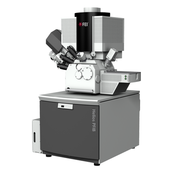
The instrument is an FEI Helios NanoLab 600i DualBeam SEM/FIB, equipped with a focused Ga+ ion beam (known as “Tomahawk”) and a high-resolution field emission scanning electron (“Elstar”) column. This setup is enhanced by improvements in patterning, scripting, and various accessories. Together, these elements enable standard laboratory applications such as milling, imaging, analysis, and sample preparation at the nanoscale.
Key Features
- Material Science: Researchers use the DualBeam to study the microstructure of materials, analyze phase distributions, and investigate the properties at the micro and nano scales. It’s especially useful for understanding metals, ceramics, and composites.
- Semiconductor Manufacturing: The instrument is crucial for defect analysis, circuit edit, and failure analysis within semiconductor manufacturing. It allows for precise material removal and deposition which is essential for device modification and troubleshooting.
- Biology and Life Sciences: In life sciences, the DualBeam can be used for ultra-structural studies of biological samples. It helps in preparing and analyzing sections of tissues or cells at nanometer resolutions.
- Geology and Mineralogy: Geoscientists use the DualBeam to examine the fine structure of minerals and rocks. This can be particularly useful for understanding the crystalline structures and chemical compositions of geological samples.
- Nanotechnology: The instrument is key in fabricating and manipulating nanostructures. It can be used for prototyping micro and nano devices, such as sensors, and for developing new materials with novel properties.
- Forensics: In forensic science, the DualBeam helps in the detailed analysis of samples such as fibers, fragments, or residues, providing crucial information for investigations.
- Cultural Heritage: Conservators and researchers use the DualBeam to study the materials and techniques used in historical artifacts, helping in preservation and restoration efforts.
Specifications
- Elstar UHR immersion lens FESEM column
- Accelerating voltage range: 0.35 – 30 kV
- Beam deceleration with stage bias from -50 V to -4 kV
- Landing voltage range 20 V – 30 kV
- Probe current range: 0.7 pA to 22 nA
- Electron beam resolution at optimum WD
- 0.8 nm at 30 kV (STEM)
- 0.9 nm at 15 kV
- 1.4 nm at 1 kV
- Electron beam resolution at coincident point
- 0.9 nm at 15 kV
- 1.6 nm at 5 kV
- 2.5 nm at 1 kV
- Tomahawk ion column
- Accelerating voltage range: 0.5 – 30 kV
- Probe current range: 0.1 pA – 65 nA with 15 apertures
- Time-of-flight (TOF) correction
- Ion beam resolution at coincident point
- 4.0 nm at 30 kV using preferred statistical method
- 2.5 nm at 30 kV using selective edge method
- High precision 5-axes motorized stage
- XY: 150 mm, piezo-driven
- Z: 10 mm, motorized
- T: -10º – 60º
- R: n x 360º (endless), piezo-driven
- Tilt accuracy (between 50º to 54º): 0.1º
- X, Y repeatability: 1.0 µm
- Detectors
- Elstar in-lens SE detector (TLD-SE)
- Elstar in-lens BSE detector (TLD-BSE)
- Everhart-Thornley SE detector (ETD)
- IR camera for viewing sample/column
- Door-mounted Nav-Cam
- High performance Ion Conversion and Electron (ICE) detector for secondary ions (SI) and electrons (SE)
- Retractable low voltage, high contrast solid-state electron detector (DBS)
- Retractable STEM detector with BF/DF/HAADF segments
- Beam current measurement
- Chamber
- 4mm E- and I-beam coincidence point at analytical WD
- Angle between electron and ion columns: 52º
- Maximum sample size: 150 mm diameter with full rotation
- Maximum clearance between stage and coincidence point: 55 mm
- Sample Weight: maximum 500 g (including the sample holder)
- Image processor
- Dwell time range from 0.025 to 25,000 µs/pixel
- Up to 6144 x 4096 pixels
- SmartSCAN (256 frame average or integration, line integration and averaging, interlaced scanning) and DCFI (Drift Compensated Frame Integration)